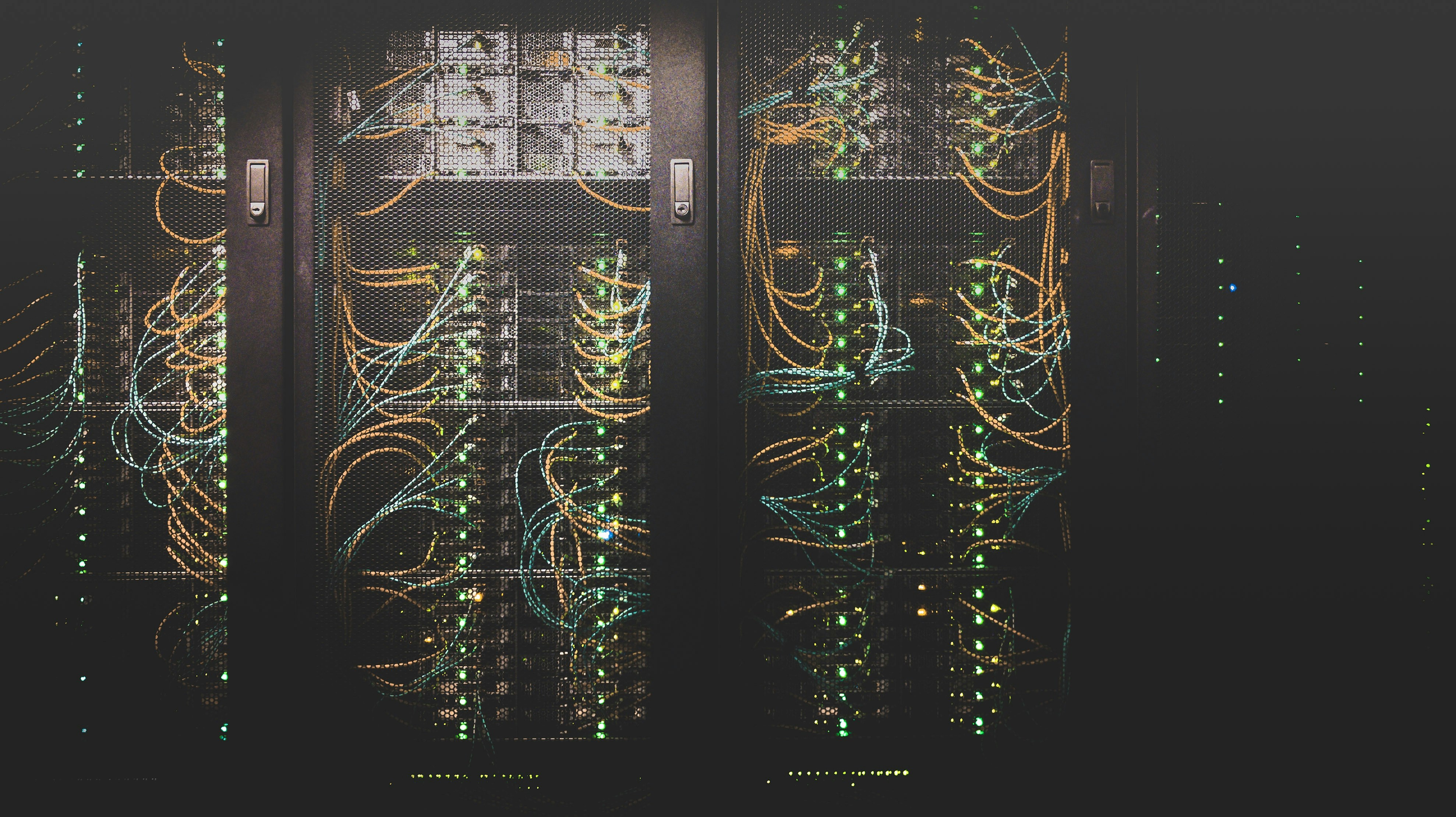
The United Arab Emirates has unveiled what is now the world's largest artificial intelligence chip, an extraordinary feat of semiconductor engineering featuring an unprecedented 4 trillion transistors integrated onto a single wafer-scale processor. The breakthrough, announced at the World Governments Summit 2026 in Dubai, is the product of a strategic collaboration between Abu Dhabi-based G42 and US-based Cerebras Systems, the pioneer of wafer-scale computing technology. The chip represents not just a technological milestone but a fundamental statement of the UAE's ambitions in the global semiconductor and AI hardware landscape — domains that have until recently been the exclusive preserve of a handful of companies based in the United States, Taiwan, and South Korea.
The 4-trillion-transistor count is staggering by any measure. To put it in perspective, NVIDIA's flagship Blackwell B200 GPU contains approximately 208 billion transistors. Apple's M4 Max chip, considered one of the most advanced consumer processors available, contains roughly 28 billion transistors. The UAE's new wafer-scale engine therefore packs more transistors than approximately 20 NVIDIA flagship GPUs or 140 high-end Apple processors combined into a single unified processing unit. The implications for AI training performance, energy efficiency, and the economics of large-scale AI computing are profound, and the chip will form the technological backbone of the 5-gigawatt UAE-US AI Campus rising in Abu Dhabi.
4T
Transistors on a Single Chip
5GW
UAE-US AI Campus Capacity
10 mi²
Campus Footprint Abu Dhabi
200MW
First Cluster Live in 2026
Wafer-Scale Computing: A Different Path to AI Performance
Understanding why the 4-trillion-transistor chip represents such a significant breakthrough requires appreciating the fundamental architectural difference between wafer-scale processors and conventional GPUs. Traditional semiconductor manufacturing produces individual chips that are then connected together through circuit boards, networking switches, and inter-server communication systems to form computing clusters. Each layer of connection introduces latency, energy consumption, and complexity, and the aggregate performance of a multi-chip cluster is always less than the sum of its individual chip performances due to these communication overheads.
Cerebras pioneered the wafer-scale approach as an alternative path: rather than producing many small chips and connecting them externally, manufacture a single enormous chip that contains all the computing resources of an entire cluster on one piece of silicon. The communication paths between processing elements are dramatically shorter, the energy required to move data between them is far lower, and the system as a whole behaves as a single unified computer rather than a network of cooperating computers.
Wafer-Scale Advantage: By integrating 4 trillion transistors on a single wafer instead of distributing them across many chips, the UAE-G42-Cerebras processor eliminates the communication bottlenecks that limit conventional GPU clusters. The result is dramatically higher performance for the largest AI training workloads.
The wafer-scale approach is particularly well-suited to the largest AI training workloads, where the size of the AI model and the volume of training data exceed what can fit comfortably on smaller chips. Modern frontier AI models — including the largest language models, multimodal systems, and scientific simulations — benefit dramatically from the unified architecture that wafer-scale processors provide.
The G42-Cerebras Partnership: From Collaboration to World Leadership
The unveiling of the 4-trillion-transistor chip caps an extended period of deepening collaboration between G42 and Cerebras that has gradually moved the partnership from technology adoption to active co-development. G42 began as a major customer of Cerebras's wafer-scale processors, deploying the technology in its growing portfolio of data centres and AI computing facilities. Over time, the relationship evolved as G42 contributed to product roadmap discussions, jointly funded research efforts, and ultimately participated in the design of next-generation chips tailored to the specific demands of large-scale UAE AI infrastructure.
The new wafer-scale engine reflects this evolution. While Cerebras provides the foundational wafer-scale technology and manufacturing expertise, G42 has contributed insights derived from operating one of the world's most ambitious AI infrastructure programmes, including specific requirements for the kinds of workloads that will run on the UAE-US AI Campus. The result is a chip that is not merely the latest iteration of Cerebras's product line but a purpose-engineered solution for the strategic AI requirements of a sovereign nation building world-class AI capability.
"This collaboration represents a new model for AI hardware development. Rather than buying off-the-shelf chips from established vendors, the UAE is co-designing the silicon that will run its most strategically important AI workloads. This level of vertical integration in AI capability is something that, historically, only the very largest US technology companies have attempted."
Industry Analysis, AI Hardware Outlook 2026
The 5-Gigawatt UAE-US AI Campus: Where the Chip Will Live
The 4-trillion-transistor chip is not designed to operate in isolation but to populate the massive computing infrastructure of the 5-gigawatt UAE-US AI Campus, the joint US-UAE megaproject taking shape across 10 square miles of Abu Dhabi territory. The campus, which incorporates the Stargate UAE project announced in May 2025 with partners including OpenAI, Oracle, NVIDIA, Cisco, and SoftBank, will eventually host the largest concentration of AI computing power outside the continental United States.
The first 200-megawatt cluster within the campus is expected to go live in 2026, with additional capacity coming online in subsequent phases. The 4-trillion-transistor chips will be deployed alongside other advanced AI processors, including NVIDIA's Grace Blackwell GB300 systems, creating a heterogeneous computing environment in which different workloads can be matched to the most appropriate hardware platform. For the largest training runs and the most computationally intensive scientific applications, the wafer-scale engines will provide capabilities that conventional GPU clusters cannot match.
Strategic Implications for the UAE
The unveiling of a domestically co-developed AI chip carries significance that extends far beyond the technical specifications of the device itself. For the UAE, the achievement represents a step-change in the depth of the country's AI capability and a strategic positioning that very few nations can replicate.
Sovereignty Over AI Infrastructure
One of the most important strategic dimensions is the move toward genuine sovereignty over AI infrastructure. Countries that rely entirely on imported AI chips remain vulnerable to supply disruptions, export controls, and pricing pressures determined by foreign manufacturers. By participating in the design and co-development of advanced AI processors, the UAE reduces its dependence on any single supplier and gains influence over the technology roadmap that will shape its AI capabilities for the next decade.
Magnet for Global AI Talent and Investment
The presence of frontier AI hardware development in the UAE serves as a powerful magnet for AI talent and investment from around the world. Researchers, engineers, and companies that want to work at the cutting edge of AI hardware now have a compelling reason to consider the UAE as a destination. This talent gravity effect compounds over time, with each high-profile achievement attracting additional talent that enables further achievements.
Geopolitical Positioning
The UAE-US partnership underlying the chip development reflects the broader strategic alignment between the two countries on questions of AI leadership and technology cooperation. At a time when global technology relationships are being reshaped by geopolitical competition, the depth of UAE-US cooperation in AI hardware sends a clear signal about which technological ecosystem the UAE is choosing to build its future within.
Performance Capabilities: What 4 Trillion Transistors Can Do
The practical performance capabilities of the 4-trillion-transistor processor will be profound across the range of AI workloads that organisations are running today and planning for the near future.
Foundation Model Training
Training the largest AI foundation models — including modern large language models with hundreds of billions of parameters, multimodal models combining vision, language, and audio, and the next generation of frontier AI systems — requires extraordinary amounts of computing power and the ability to maintain high utilisation across that compute. Wafer-scale processors are particularly effective at this kind of workload, with recent benchmarks showing that Cerebras systems can train models several times faster than equivalent GPU clusters for comparable price points.
Scientific Simulation
Beyond traditional AI applications, wafer-scale processors are increasingly being deployed for scientific simulation in fields including climate modelling, drug discovery, materials science, and computational physics. The unified memory and compute architecture of wafer-scale chips makes them well suited to scientific workloads that require complex data flows and large working memory, often outperforming specialised supercomputers built from many discrete components.
Real-Time Inference at Scale
For deployment of AI systems at scale, where many concurrent users are accessing AI capabilities simultaneously, the wafer-scale architecture enables impressive throughput characteristics. Single chips capable of supporting thousands of concurrent inference requests can dramatically reduce the data centre footprint and energy consumption required to deploy AI services at scale.
The Manufacturing Achievement
Manufacturing a chip with 4 trillion transistors is itself an extraordinary feat that places the UAE-G42-Cerebras collaboration alongside the most technologically sophisticated organisations in the world. Conventional chip manufacturing achieves yields by producing many small chips on each wafer, then discarding the chips that contain manufacturing defects. Wafer-scale processors instead use the entire wafer as a single chip, requiring novel approaches to handle defects that would be acceptable in conventional manufacturing but catastrophic for a wafer-scale design.
Cerebras pioneered the techniques for this manufacturing approach, including redundant compute resources that can be activated to replace defective elements, novel interconnect architectures that maintain high yields despite defects, and packaging and cooling systems specifically designed to handle the unique thermal challenges of an active silicon wafer. The 4-trillion-transistor chip represents the latest evolution of these techniques, pushed to scales that were considered impossible just a few years ago.
Energy Considerations
The energy footprint of a chip with 4 trillion transistors is substantial, and the UAE's commitment to sustainable AI infrastructure development means that significant attention has been paid to power efficiency, cooling, and renewable energy integration. The wafer-scale architecture itself is generally more energy-efficient than equivalent GPU clusters because the elimination of inter-chip communication reduces the energy spent moving data around. However, packing 4 trillion transistors onto a single device still consumes considerable power that must be sourced and dissipated effectively.
The 5-gigawatt UAE-US AI Campus has been designed with sustainability considerations from the outset, incorporating renewable energy sourcing, advanced cooling technologies, and integration with the UAE's broader clean energy strategy. As the campus comes fully online over the next several years, the combination of advanced silicon and clean infrastructure will serve as a model for sustainable large-scale AI deployment.
Broader Implications for the AI Hardware Landscape
The UAE's entry as a frontier player in AI hardware has implications for the global semiconductor and AI computing landscape that extend well beyond the country itself. The successful co-development of a world-leading chip outside the traditional centres of US, Taiwanese, and South Korean semiconductor expertise demonstrates that the geography of AI hardware leadership is becoming more distributed.
Other nations watching the UAE's example may be encouraged to pursue similar strategies — partnering with established semiconductor companies to co-develop chips tailored to national strategic requirements rather than relying entirely on imports. This could accelerate the diversification of the AI hardware landscape, eventually producing a more competitive market with multiple credible suppliers offering distinct architectural approaches.
For NVIDIA, which currently dominates the AI training hardware market, the rise of credible alternatives like the UAE-G42-Cerebras wafer-scale processor represents both competitive pressure and opportunity. While NVIDIA remains the dominant player and is itself an active partner in UAE AI infrastructure projects, the existence of differentiated alternatives benefits the broader AI ecosystem by providing customers with options matched to their specific requirements.
Looking Forward: The Road From Unveiling to Deployment
With the chip unveiled at WGS 2026, attention now turns to the practical work of deploying the technology at scale within the UAE-US AI Campus and other UAE AI facilities. The first 200-megawatt cluster going live in 2026 will provide the initial real-world deployment, with subsequent phases expanding the deployment footprint substantially.
For researchers and AI companies operating in the UAE, the availability of frontier wafer-scale computing represents a genuine advantage that will enable work at the cutting edge of AI research and development. Whether training the next generation of foundation models, conducting large-scale scientific simulations, or deploying AI services to millions of users, the access to world-leading hardware that the UAE is building will support work that simply could not be done elsewhere with the same efficiency and capability.
The 4-trillion-transistor chip is, in many ways, a tangible expression of the UAE's broader AI ambitions: not merely participating in the global AI economy as a customer of foreign technology, but actively shaping the technology itself and using that capability to build sovereign AI infrastructure capable of competing with the largest deployments anywhere in the world. As more chips are manufactured, deployed, and put to use in real applications, the practical implications of this strategic positioning will become increasingly visible — and the UAE's status as a global AI hardware power will be cemented.
Frequently Asked Questions
What is the world's largest AI chip?
The chip unveiled at WGS 2026 is a wafer-scale processor co-developed by G42 and Cerebras Systems, featuring 4 trillion transistors integrated on a single wafer. This is roughly 20 times the transistor count of NVIDIA's flagship Blackwell B200 GPU and represents the largest single AI chip ever produced.
How does wafer-scale computing differ from conventional chips?
Conventional chips are produced as small individual processors and connected externally through circuit boards and networks. Wafer-scale processors integrate the entire computing capability onto a single piece of silicon, eliminating the communication bottlenecks that limit conventional GPU clusters. This produces dramatically higher performance for the largest AI workloads.
Where will the chips be deployed?
The 4-trillion-transistor chips will populate the 5-gigawatt UAE-US AI Campus in Abu Dhabi, which spans 10 square miles. The first 200-megawatt cluster will go live in 2026, with additional phases bringing the campus to full capacity in subsequent years. This will be the largest concentration of AI computing power outside the United States.
What is G42's role in this development?
G42 has evolved from being a major customer of Cerebras to actively co-developing chips tailored to UAE strategic requirements. The Abu Dhabi-based AI company contributes operational insights from running one of the world's most ambitious AI infrastructure programmes, helping shape silicon designs specifically for sovereign-scale AI workloads.